


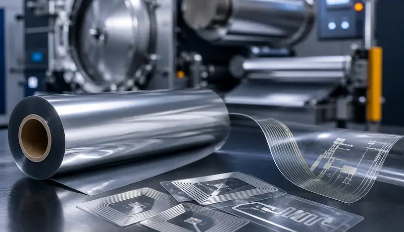
RFID Antennas and Printed Electronics: Metallized Film as a Conductive Substrate
Every RFID tag, NFC sticker, and printed sensor carries a conductive pattern that either captures radio waves or carries a signal. However, that pattern needs a substrate that conducts well, bends without cracking, and costs little. For decades, manufacturers relied on etched copper and aluminum foil, and later on printed silver ink. Today a third option is gaining ground: metallized film for RFID antennas.
Metallized film pairs a thin polymer carrier with a vacuum-deposited metal layer, so it works as a lightweight conductive substrate. In this guide, we explain how it compares with foil and conductive inks, how manufacturers pattern it into antennas, and what a vacuum metallizer must deliver to coat it reliably.
What RFID Antennas and Printed Electronics Demand From a Substrate
RFID spans several frequency bands, and each one shapes the antenna. Low-frequency tags (125 kHz) use wound coils, high-frequency tags (13.56 MHz) cover NFC, and ultra-high-frequency (UHF) tags operate near 860–960 MHz with a read range of 2–8 meters. Regardless of band, the substrate must meet the same core demands:
- Low sheet resistance — a conductive pattern loses energy as resistance rises, and that loss shortens read range.
- Flexibility and crease resistance — tags bend, fold, and laminate onto curved packaging, so a brittle conductor cracks and fails.
- Thin, light construction — thin inlays disappear inside labels and hangtags, and they use less material.
- Strong adhesion — the metal layer must survive slitting, lamination, and printing without lifting.
- Low cost per square meter — RFID and smart labels sell in huge volumes at low prices, so material cost dominates.
Consequently, antenna makers look for a conductor that balances conductivity against cost, thickness, and flexibility. That trade-off explains why metallized film for RFID antennas now attracts attention.
How Metallized Film Works as a Conductive Substrate
Vacuum metallizing deposits a thin aluminum layer — or copper in some designs — onto a PET or BOPP web inside a roll-to-roll chamber. Moreover, the operator controls layer thickness by monitoring optical density or sheet resistance, so the process holds the conductor within a narrow tolerance across the full web width.
Three properties make this approach attractive for antennas and printed electronics:
- Uniformity: a vacuum-deposited layer covers the web evenly, so every antenna on the roll starts from the same resistance.
- Thinness and flexibility: a sub-micron metal layer flexes with the polymer and survives converting without cracking.
- Process simplicity: the vacuum route avoids wet chemistry, and it scales through the same roll-to-roll platforms that coat packaging film.
One trade-off deserves emphasis. Because sheet resistance equals resistivity divided by thickness, a thinner metal layer raises sheet resistance. In practice, a 0.5 µm aluminum layer sits near 50–60 mΩ/sq, while a 9 µm foil sits near 3 mΩ/sq (a simple ρ/t calculation). In addition, skin effect matters at UHF: the current concentrates in the top few micrometers of the conductor, so extra aluminum thickness adds cost without adding much conductivity. Therefore, designers pick a layer that matches their read-range target rather than simply maximizing thickness.
Metallized Film vs Foil and Conductive Inks
Metallized film therefore sits between solid metal foils, which offer the highest conductivity, and conductive inks, which trade conductivity for printability. It wins on cost, thinness, and process simplicity — the exact qualities that high-volume tags reward. For reference, published research on screen-printed antennas reports silver-ink sheet resistance below 5 mΩ/sq after sintering, which shows how quickly ink chemistry keeps improving.
Patterning the Antenna: Etching, Laser Ablation, and Selective Coating
A continuous conductive layer does not make an antenna; the manufacturer must shape it. Antenna makers use several routes, and each one suits a different product:
- Chemical etching — the classic method, which uses a resist and an etchant to dissolve unwanted metal. Etching works well, yet it consumes chemicals and generates wastewater; starting from a thin metallized layer reduces both the etch time and the waste.
- Laser ablation — a laser scribes the thin metal directly, which removes the wet process entirely and suits metallized film with thin layers.
- Selective or masked deposition — the coater deposits metal only where the antenna needs it, which cuts material waste but demands tighter process control.
- Transfer and demetallization — for labels, transfer metallization plus selective demetallization builds the pattern during converting.
Because a conductive substrate controls only the raw conductivity, the patterning step decides antenna geometry and read performance. A smart buyer therefore evaluates the film and the patterning route together.
Where Metallized Film Fits
Manufacturers apply metallized film for RFID antennas across several product families:
- HF and NFC tags and stickers — thin, flexible antennas for cards, labels, and wearables.
- UHF tags — where cost and thinness matter more than maximum read range.
- EAS security labels — anti-theft labels that need a low-cost resonant circuit.
- Smart and active labels — packaging-embedded antennas that pair with freshness sensors, NFC engagement tags, and QR experiences.
- Flexible printed electronics — membrane switches, sensors, and simple circuits that need a conductive base layer.
Meanwhile, long-range UHF tags still favor thicker aluminum or copper, because their link budget demands the lowest possible resistance. Consequently, the right choice depends on the read-range target, not on a single universal rule.
What to Look For in a Vacuum Metallizer
Coating RFID antenna film rewards precision, because a poor layer wastes an expensive downstream process. Therefore, buyers should weigh these machine capabilities:
- Gentle web handling with stable tension — thin PET and BOPP webs wrinkle and stretch, so tension control protects conductivity uniformity.
- Uniform deposition across the width — variation across the web shifts sheet resistance from antenna to antenna.
- Inline resistance or OD monitoring — closed-loop control keeps the layer on target roll after roll.
- Multi-metal capability — aluminum, copper, and silver cover different antenna designs and frequencies.
- Patterning options — selective coating or a downstream etch or laser step defines the antenna geometry.
- A clean, high-vacuum chamber — particles and pinholes break antenna continuity and kill read range.
A platform such as Tempo Machinery’s fully automatic suspension vacuum coating machine combines a free-suspension web path, double coating-drum cooling, online OD detection, a Siemens PLC, and four servo motors that hold constant tension. For copper layers, the induction heating metallized machine and our sputtering capability extend the material range. In practice, our standard machines cover 6–150 µm, while some antenna films run thinner, so we always recommend discussing your exact RFID antenna film and resistance target with our engineers before you order.
Quality Checks That Decide Tag Performance
Because the antenna lives or dies by its conductivity, quality control for metallized film for RFID antennas differs from packaging-film inspection.
Because adhesion and pinholes cause most field failures, our guides to adhesion testing for metallized film and vacuum coating defect troubleshooting help operators set practical limits. For a close look at how thin metal layers behave as electrodes, see our article on metallized film for capacitors.
Market Outlook for RFID and Printed Electronics
Demand keeps rising on both sides of this application. Wikipedia’s overview of RFID reports that the market value should climb from about $12.08 billion in 2020 to $16.23 billion by 2029, and that vendors sold roughly 50 billion tag chips in 2024. Furthermore, the printed-electronics market supports the trend: Technavio estimates growth of $68.68 billion at a 17.92% CAGR from 2023 to 2028, while SNS Insider values flexible electronics at $32.65 billion in 2023 and projects $75.04 billion by 2032.
As brands embed antennas into packaging for inventory, authentication, and engagement, the conductive substrate becomes a volume material. That shift favors low-cost, roll-to-roll RFID antenna film produced by vacuum metallizing, including metallized film for RFID antennas.
Conclusion
Metallized film for RFID antennas gives tag makers a lightweight conductive substrate that balances conductivity, flexibility, and cost. It cannot match thick copper foil for every long-range UHF design, yet it beats foil on thinness and process simplicity, and it beats printed silver on cost. However, the application demands uniform deposition, disciplined tension control, and tight quality checks. Therefore, choose equipment built for thin-film precision, and verify sheet resistance before you commit to volume production.
Ready to evaluate a vacuum metallizer for RFID antenna film? Contact our team for machine specifications, customization options, and a free consultation on your coating requirements.
FAQ
1. Can metallized film replace copper or aluminum foil in RFID antennas?
Partly. Metallized film suits HF, NFC, EAS, and many cost-driven UHF designs. Long-range UHF tags usually keep thicker aluminum or copper, because their link budget needs the lowest sheet resistance.
2. Why does sheet resistance matter for an RFID antenna?
Sheet resistance sets how much energy the antenna loses as current flows through it. Lower resistance means less loss, more radiated power, and a longer read range, so antenna designers treat it as a primary specification.
3. How do manufacturers pattern a metallized film into an antenna?
They use chemical etching, laser ablation, selective or masked deposition, or transfer and demetallization. Laser ablation and selective coating avoid wet chemistry, which makes them attractive for thin metallized layers.
4. Which vacuum coating method suits RFID antenna film?
Thermal evaporation handles aluminum well, and it covers most RFID and NFC antenna film. Copper designs use electron-beam evaporation or magnetron sputtering, because copper melts at a much higher temperature.
5. Is metallized film suitable for printed electronics beyond RFID?
Yes. The same conductive substrate serves membrane switches, sensors, and simple flexible circuits. Any application that needs an even, thin, low-cost conductor can benefit from vacuum metallizing.